Tuesday, 9 January 2018

// // Leave a Comment

Last Year Paper of BUSINESS COMMUNICATION of Uttarakhand Technical University UTU

Last Year Paper of BUSINESS COMMUNICATION of Uttarakhand Technical University UTU 
you can find Last year question paper and study notes of Uttarakhand Technical University (UTU) here 

Last Year Paper of BUSINESS COMMUNICATION UTU 
B.C.A First Semester Examination-2018
Business Communication


Time Duration: Three Hours 
Total Marks: 70 

Instruction: Attempt any five questions. All questions carry equal marks.

Q1.  What is perceptual organization? Discuss Gestalt’s laws of

        perceptual organization.

Q2.  Discuss the cognitive theory of learning. Also delineate the

        differences between Behavioral school and cognitive schools

        of learning.

Q3.  What is Motivation? Discuss various theories of Motivation 

        and  how they are important in learning?                                    

Q4.  What do you mean by communication? Discuss various barriers

        to the communication.

Q5.  What is written communication? Discuss the various advantages

        written communication has over oral communication.

Q6.  Discuss various techniques and methods used for the appraisal

        or assessment of personality.

Q7.  Define any of the five terms:

       a). Perception

       b). Social learning theories

       c). Upward communication

       d). Personality

       e). Public Speaking

       f). Needs for motivation

       g). Ingredients of successful presentation
Read More

Sunday, 7 January 2018

// // Leave a Comment

MICROPROCESSOR 2013, B.Tech 4th Semester exam paper of Uttarakhand Technical University


MICROPROCESSOR 2013, B.Tech 4th Semester exam paper of UTU


MICROPROCESSOR
SEM-IV, 2013
B.TECH EXAMINATION
UTTARAKHAND TECHNICAL UNIVERSITY
utu previous question paper

Time: 3 Hours
Total Marks: 100
Attempt any four questions 
4*5=20
  1. Explain the various types of microprocessor with its evolution period.
  2. Explain the difference between processor and microcontroller.
  3. Explain the interrupt structure of 8279.
  4. Explain the addressing mode of 8085 with suitable examples.
  5. Explain the importance of USB for data transfer.
  6. Draw the block diagram of 8255 and how it differs from 8251, explain.
Attempt any four questions
4*5=20
  1. Draw and explain the pin diagram of 8086.
  2. What are the various status flags provided in 8085? Discuss their role in details.
  3. Discuss the principle of A/D convertor with suitable example.
  4. Draw and explain the timing diagram of opcode fetch cycle.
  5. Explain with examples CALL, RETURN, PUSH and POP instructions.
  6. Explain the flag register and various interrupts of 8086.
Attempt any two questions
2*10=20
  1. What is emulator? Explain how a DAC can be interfaced to an Intel 8087.
  2. Explain the different addressing mode, timer and register bank of 8086 with suitable example.
  3. Differentiate static and dynamic memory? Explain how you can interface 128K byte memory with 8086.
Attempt any two questions 
2*10=20
  1. Justify, why 8251 called as USART? Define the mode word register of 8251 for asynchronous mode.
  2. What are the maskable and non-maskable interrupts? Discuss AHOLD, BREQ and BOFF signals of 80486.
  3. Define the interrupt priority of 8051? Explain the assembler directives, Macros, PROM, SRAM and locator with suitable examples.
Attempt any two questions
2*10=20
  1. What is debugger? Draw and explain the block diagram of keyboard display controller (8279).
  2. Draw the block diagram of 8254 and discuss the default state of 8254 upon power up or reset state.
  3. What is PCI? Write an 8086 program to transfer a block of data. The data is stored in memory from C550H to C55FH. The data is to be stored from C550H to C57FH in reverse order.
Read More
// // Leave a Comment

COMPUTER ORNANIZATION 2013, B.Tech 4th Semester exam paper of Uttarakhand Technical University

COMPUTER ORNANIZATION 2013, B.Tech 4th Semester exam paper of UTUCOMPUTER ORGANIZATION


SEM-IV, 2013
B.TECH EXAMINATION
UTTARAKHAND TECHNICAL UNIVERSITY
(UTU)

Time: 3 Hours
Total Marks: 100
Attempt any four:
4×5=20
  1. List the major component of computer organization and explain in detail.
  2. Explain the IEEE standard for floating point numbers with suitable examples.
  3. Explain the function of control unit and Instruction format in details.
  4. What is RISC? Draw and explain the Berkeley RISC I instruction format.
  5. Explain the importance of HOLD and HLDA pin data transfer through DMA.
  6. Draw the block diagram of multiprocessor and explain the role of cache coherence in processor.
Attempt any four:
4×5=20
  1. How many switch points are there in a crossbar switch network that connects p processor to m memory modules?
  2. Design an array multiplier that multiplies two 4-bit numbers by using AND gates and binary adders.
  3. What is difference between isolated I/O and memory mapped I/O and also explains the advantages and disadvantages of each.
  4. Calculate the address lines for 8 bytes memory.
  5. Determine the number of clock cycles that it takes a process 200 tasks in a six segment pipeline.
  6. What are the basic difference between a branch instruction, a call subroutine instruction and program interrupt?
Attempt any two:
2×10=20
  1. What is RTL? Represent the number(+46.5)10 as a floating point binary number with 24 bits. The normalized fraction mantissa has 16 bits and the exponent has 8 bits.
  2. Explain the different arithmetic and logic micro-operations. Draw and discuss the 4 bit arithmetic circuit in detail.
  3. Explain the difference between hardwired and micro programmed control unit in detail.
Attempt any two:
2×10=20 
  1. Define addressing mode? Write the RISC I instruction in assembly language that will cause a jump to address 3200 if the Z (zero) status bit is equal to 1 by using immediate mode.
  2. What is instruction pipelining? Consider the multiplication of two 40×40 matrices using a vector processor. Find out how many product terms are there in each inner product and how many inner products must be evaluated.
  3. Define the mode of information transfer? Draw and explain the priority interrupt hardware by using four interrupt sources.
Attempt any two:
2×10=20

  1. Draw and explain the block diagram of DMA controller and DMA transfer mechanism.
  2. Explain the various characteristic of multiprocess? or Construct a diagram for a 4×4 omega switching network. Show the switch setting required to connect input 3 to output 1.
  3. Explain memory hierarchy in a computer system? A digital computer has a memory unit of 64K×16 and a cache uses direct mapping with block size of four words. Find out the total numbers of bits in the tag, index, block and word fields of the address format.
Read More
// // Leave a Comment

FUNDAMENTAL OF ELECTRONICS ENGINEERING 2013, B.Tech 2nd Semester exam paper of Uttarakhand Technical University

FUNDAMENTAL OF ELECTRONICS ENGINEERING 2013, B.Tech 2nd Semester exam paper of UTU


FUNDAMENTAL OF ELECTRONICS ENGINEERING

SEM-II, 2013

B TECH QUESTION PAPER

UTTARAKHAND TECHNICAL UNIVERSITY


Time: 3 Hours
Total Marks: 100
Attempt any four parts of the following:
  1. Define Semiconductor materials on the basis of energy band diagram with an example.
  2. How electron-hole pairs are generated. Explain the working of different forms of semiconductors.
  3. Why Si is preferred over Ge for manufacturing of electronics devices. How Semiconductors diode behaves as the switch.
  4. Explain the effect of temperature on I-V characteristics of the p-n junction diode.
  5. Differentiate between extrinsic and intrinsic semiconductor on the basis of impurity present in them.
  6. Explain the working of Semiconductor diode at different biasing conditions, no bias, forward bias & reverse bias condition.
Attempt any four parts of the following:
  1. Explain full wave bridge rectifier.
  2. Prove that efficiency of full wave rectifier is 81%.
  3. The reverse saturation current of a silicon diode in 3 nA at 27oC find-
    (i) Reverse saturation current at 82o
    (ii) Forward current at 82o C if the forward voltage applied is 82o C.
  4. Sketch Vo for the circuit shown below D1 and D2 are silicon diodes.
    utu previous year question paper Electronics
  5. Determine Vfor network given below.
    utu previous year question paper Basic Electronics
  6. Explain Voltage Doublers or Voltage Tripler with neat diagram.
Attempt any two parts of the following:
  1. (i) Explain Zener diode, draw its symbol and V-I characteristics.
    (ii) In a Zener voltage Regulator find the range of RLand IL for Load voltage to be constant.
    utu previous year question paper Basic Electronics
  2. Draw a Voltage Regulation that will maintain an output voltage of 20V across a 1KΩ load with an input that will vary between 30 and 50 V. That is determining the proper value of series Resistance (Rs) and maximum current IZM.
  3. Explain Zener Diode application as the shunt regulator.
Attempt any two parts of the following:
  1. (i) Derive the relation between α & β of the transistor, also calculate β for given α= 0.95.
    (ii) Explain potential divider biasing of the transistor.
  2. (i) Explain the working of NPN transistor at no bias and active mode condition.
    (ii) What is closed loop non-inverting amplifier, derive an expression for it.
  3. (i) The BJT amplifier has hfe= 100, VBE = 0.007 V, ICO = 0. Calculate the value of R1 and RC. Such that IC =1 mA and VCE = 2.5V.
    utu previous year question paper Basic Electronics
    (ii) For the following, as shown in the following, determine the output voltage vo if the input voltage vi = 1.2 V.
    utu previous year question paper
Attempt any two parts of the following:
  1. (i) Write down characteristics of ideal OP-AMP.
    (ii) What is close loop non inverting amplifier, derive expression for it.
  2. (i) Convert the following numbers:
    (a) (4021.25)10= ( )2
    (b) (101010.10)4 = ( )8
    (c) (23.AB)16 = ( )2
    (d) (111011)2 = ( )gray code
    (v) (23.53)10 + (23.58)8 = ( )10
    (ii) Minimize the following Boolean function and draw its logic diagram using minimum universal gates.
  3. Explain the construction and working of n-channel enhancement type MOSEFET. Also draw its drain and transfer characteristics of the same.
Read More

Saturday, 6 January 2018

// // Leave a Comment

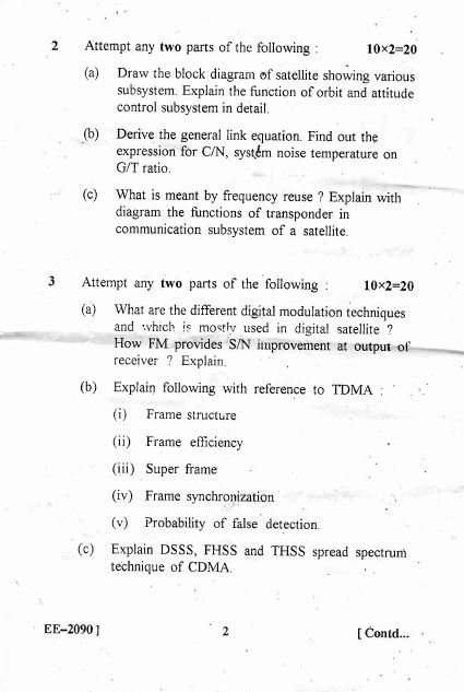
SATELLITE-COMMUNICATION 2010, 7th Semester B.Tech exam paper of Uttarakhand Technical University

UTU B.Tech Previous year exam paper of SATELLITE-COMMUNICATION 2010, 7th semester


Read More
// // 1 comment

Uttarakhand Technical University B.Tech exam paper of OPTICAL FIBER COMMUNICATION SYSTEM 2012, 7th Semester

UTU B.Tech Previous year exam paper of OPTICAL FIBER COMMUNICATION SYSTEM 2012, 7th semester


OPTICAL FIBER COMMUNICATION SYSTEM
SEM-VII, 2012-13
B.TECH EXAMINATION
UTTARAKHAND TECHNICAL UNIVERSITY

Time: 3 Hours
Total Marks:100
Attempt any four parts:
  1. Discuss Dispersion mechanism with respect to single mode fiber indicating the dominating effects and then show how inter-modal dispersion may be minimize within the single mode region.
  2. Briefly discuss with the aid of a suitable diagram what is meant by the acceptance angle for an optical fiber. Show how this is related to the fiber numerical aperture and the refractive indexes for the fiber core and cladding?
  3. A step index with a large core diameter compared with the wavelength of the transmitted light has an acceptance angle in air of 22 degree and a relative refractive index difference of 3%. Estimate the numerical aperture and the critical angle at the core-claddinginterface of the fiber.
  4. What are the modes in optical fiber? Calculate number of modes for a graded index optical fiber if core diameter (d = 62.5 μ m), NA =0.275 and Operating wavelength = 1300 nm.
  5. Two polarization maintaining fibers operating at the wavelength of 1.3 micrometer have beat length of 0.7 mm and 0.8 mm. Determine the briefringence in each case and comment the result.
  6. Derive an expression for the acceptance angle for skew rays which changes direction by an angle of 2γ at each reflection in step index fiber in terms of NA and γ.
Attempt any four parts:
  1. Explain how the optical and electrical confinement is achieved in a LASER.
  2. List the three major cause of attenuation in an optical fiber and explain their mechanism.
  3. What is the difference between a surface emitting LED and edge emitting LED? An injection loss has a total efficiency in a GaAs active region as 20%. The volume applied to the device is 2.2 V and the band gap energy of GcAs is 1.43 ev. Find the external power efficiency of the device.
  4. Explain the basic construction of Laser diode and also discuss Einstein's relation with suitable expression.
  5. What are the advantages of S C laser over LED for communication and explain the mechanism of light from LED.
  6. Explain modulation bandwidth of an LED with the help of suitable frequency response curve, clearly marking optical and electrical bandwidth.
Attempt any two parts:
  1. Explain the working of a P-I-N photodiode. Also explain the factors that limit the speed of response of photodiode.
  2. Explain the impact ionization in avalanche photodiodes. Define photo multiplication factor and cutoff over length of photodiode.
  3. Discuss the expression for the SNR in an APD receiver. How the signal to noise ratio may be modified to give the optimum avalanche multiplication factor.
Attempt any two parts:
  1. Explain the necessity of preamplifier in an optical receiver. Mention the types of preamplifier used and explain the working of any one of them.
  2. Describe surface LED and PIN photodiode always operative in reverse bias region.
  3. Explain the various noise and disturbances associated with signal detection in optical receiver. Briefly discuss Quantum noise and consider this phenomenon with respect to digital signaling.
Attempt any two parts:
  1. Describe the optical power budgeting for digital optical fiber systems.
  2. How internal and external quantum efficiency is laser diode. Determine and describe Quantum well laser.
  3. Draw the block diagram of detection principle of coherent optical fiber systems.
Read More
// // Leave a Comment

Uttarakhand Technical University B.Tech exam paper of POWER ELECTRONICS2012, 6th Semester

UTU B.Tech Previous year exam paper of POWER ELECTRONICS 2012, 6th semester 


POWER ELECTRONICS
SEM-VI, 2012
B.TECH EXAMINATION
UTTARAKHAND TECHNICAL UNIVERSITY

Time: Hours
Total Marks: 100
Note: Attempt all question. Use of calculator is permitted.

Answer any four parts of the following:
  1. What are the different methods of firing employed for SCR triggering? Explain UJT firing circuit with relevant waveforms.
  2. Discuss the two transistor model of thyristor and derive an expression for the anode current.
  3. Draw the static V-I characteristics of SCR and explain its mode of operation.
  4. Name the different power electronic converters available and list their advantages over conventional modes of conversion and control.
  5. What are the characteristics of n ideal power switching device? Compare the characteristics of IGBT and MOSFET.
  6. Draw & Explain the circuit diagram for turning on & Turning off operation of a G.T.O.
Answer any four parts of the following:
  1. Define di/dt and dv/dt rating of SCR. How is SCR protected against these?
  2. For what type of protection a snubber circuit is used and discusses the design of snubber circuit.
  3. A number of SCRs, each of rating 2000 V and 50A, are to be used in series-parallel combination in a circuit to handle 11Kv and 400A. For a derating factor of 0.15, calculate the number of SCRs in series and parallel units. The maximum difference in their reverse recovery charge in 20μC. Calculate the value of dynamic equalizing capacitance.
  4. The resonant pulse communication circuit has C = 20μF and L = 5μH. Initial voltage across capacitor is Vs = 230V. For a constant load current of 300A, calculate
    (a) Conduction time for the auxiliary thyristor
    (b) Voltage across the main thyristor when it gets commutated and
    (c) The circuit turn off time for the main thyristor.
  5. Give the working of step down chopper and derive expression for output voltage.
  6. A step up chopper has input voltage of 220V and output voltage of 660 V. If the conducting time of thyristor-chopper is 100μs, compute the pulse width of output voltage. In case output voltage pulse width is halved for constant frequency operation, find the average value of new output voltage.
Answer any two parts of the following:
  1. Discuss the working of single phase full wave ac-dc convertor taking into account the effect of source inductance. Draw the output voltage waveform for firing angle 30o if overlap angle is 15o for zero degree firing angle.
  2. A 3-phase full converter, fed from 3-phase, 400V, 50 Hz source, is connected to load R = 10, E = 350 V and large inductance so that output current is ripple free. Calculate the power delivered to load and input pf for
    (a) firing angle of 30o and (b) firing advance angle of 60o.
  3. For a 3-phase semi converter, draw the output voltage waveform for a firing angle delay of 90o indicating the conduction of its various elements on the assumption of continuous output current. Discuss whether freewheeling diode comes into play or not. Also obtain the expression for output voltage.
Answer any two parts of the following:
  1. Describe the operation of a single phase full wave ac regulator feeding a resistive load. Also derive the expression for output voltage.
  2. A six pulse cycloconverter, fed from 3-phase, 400V, 50 Hz source, is delivering a load current 40 A to a 1-phase resistive load. The source has an inductance of 1.2 mH per phase. Calculate the RMS value of load voltage for firing angle delays of
    (a) 0o
    (b) 30o
  3. Describe the principle of working of single phase to single phase step down cycloconverter both continuous and discontinuous conditions for a bridge type cycloconverter.
Answer any two parts of the following:
  1. Discuss the principle of working of a three phase bridge inverter with an appropriate circuit diagram. Draw phase & line voltage waveforms on the assumption that each thyristors conducts for 180o and the resistive load is star connected. The sequence of firing of various SCRs should be indicated in the diagram.
  2. Describe how multiple pulse waves can be generated from carrier and reference waves. Hence show that
    (a) Number of pulses per half cycle, N = ωc/2ω
    (b) Pulse Width 2d/N = (1 - Vr/Vc)π/n
    where Vc & Vr are the amplitudes of carrier and reference signals respectively.
  3. For a single phase full bridge inverter, Vs = 230 V dc, T = 1ms. The load consist of RLC in series with R = 1, ωL = 6Ω and 1/ωC =7Ω
    (a) Sketch the waveform for load voltage VO fundamental component of load current i, source current is and voltage across thyristor. Indicate the device under conduction during different Interval of one cycle.
    (b) Find the power delivered to load due to fundamental component.
Read More